半导体与电子 | PerkinElmer
PerkinElmer
Semiconductor & Electronics Analysis

半导体与电子

我们提供的电感耦合等离子体质谱(ICP-MS)可最大程度消除干扰,将BEC值降至PPt级。

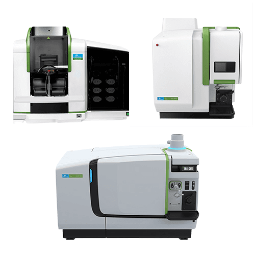
珀金埃尔默的NexION®350电感耦合等离子体质谱仪凭借其独特性能,极大地延长仪器的正常运行时间并提高了生产效率,使其成为半导体行业的首选分析仪器。与市场其他电感耦合等离子体质谱仪相比,NexION ICP-MS信号稳定性强、速度快且检出限低,也是其成为行业领导品牌的重要原因之一。此外NexION ICP-MS的设计能够最大程度地消除干扰,同时提供了最先进的纳米粒子软件,用于直径小于20纳米的单粒子分析,这也是NexION ICP-MS处于电感耦合等离子体质谱仪行业领导地位的最重要因素。

利用专为半导体市场测试需求而设计的系统,所有交钥匙方法以及用于客户评估的样品分析均在我们的100级半导体洁净室中进行。 这些设施使我们能够预测仪器安装后会出现的分析需求。 我们的目标是为您的实验室提供分析系统和适当的支持,帮助您的实验室获得尽可能低的检测限,实现快速检测。

珀金埃尔默为半导体实验室提供全套的仪器、产品和服务,包括:

  • 原子光谱仪(石墨炉原子吸收光谱仪、电感耦合等离子体质谱仪和电感耦合等离子体发射光谱仪)
  • 色谱仪(热脱附、气相色谱仪、气质联用仪、HPLC/UHPLC)
  • 分子光谱仪(傅里叶变换红外光谱和紫外-可见光谱仪)
  • 热分析和元素分析仪
  • 耗材
  • 维修服务,包括“交钥匙”维修协议

Symposium Hub

Visit this Hub page for access to all our videos on how to control semiconductor impurities from R&D to FAB and Back-End Assembly. Our most complete round-up of expertise at your fingertips.

了解更多

Research & Development

Semiconductor Research and Development Managers are tasked with establishing the right set of processes and selecting the right materials for the entire integrated circuitry (IC) manufacturing processes. The choices and recommendations semiconductor R&D managers deploy will impact the operation’s ability to achieve 24/7 manufacturing operations and downstream production ROI.

了解更多

Device Fabrication

Semiconductor, or IC wafer fabrication, is the front-end phase of semiconductor manufacturing where the many intricate steps introduce numerous points at which contaminations and chemicals impurities pose catastrophic risks to the semiconductor’s reliability and quality. Controlling trace metal and organic contaminates with ultra-clean processes is critical in each device fabrication step to ensure the quality and purity of the materials, gases, and fine chemicals used in manufacturing.

了解更多

QA/QC & Failure Testing

As personal technologies like smartphones, tablets, wearables, and the Internet of Things (IoT) devices become smaller and smaller, the highly integrated components within the devices need to become more and more complex. Quality assurance, quality control and failure testing are critical to the back-end phases of semiconductor and device manufacturing, because the sooner a defect can be identified and characterized, the faster production should re-start.

了解更多

Assembly & Packaging

Semiconductor, or IC packaging assembly, is an essential and complex back end phase of the semiconductor and electronic device design and manufacturing process. Contaminates introduced to wafer fabrication, component level packaging, module assembly, housing, and plastic components all affect the performance and ultimately the cost of the product. Like many other phases of semiconductor manufacturing, precise analytical sample testing is required to ensure the composition and quality of the assembly and packaging starting materials which are so critical to final device quality.

了解更多

Semiconductor & Electronics Solutions Spotlight

waterrecycling-512.jpg

Semiconductor Water Recycling: Analytical Action to Ensure Consistent Water Availability

As semiconductor science advances and the wafers become more complex - increasing volumes of water are needed for the production processes. Manufacturers must b ...
了解更多
electronic-board-recycling-512.jpg

Electronic Board Recycling with ICP-MS and ICP-OES: Smart, Sustainable - and Successful

Camston Wrather is revolutionizing waste disposal by pioneering sustainable resource recovery, especially from printed circuit boards. Discover how partnering w ...
了解更多
64052_Semicon_PDG_normalized-512.jpg

Semiconductor & Electronics Analysis Overview Flyer

Download this Flyer for an overview of PerkinElmer's analytical solutions for the Semiconductor industry. This 2-page flyer outlines semiconductor and microelec ...
了解更多
analyses-in-recycling-512x288.jpg

Analyses in Recycling: Mining Our Electronic Waste for Precious Recyclates

The MetroCycleEU (project #: 20IND01) under the umbrella of the EMPIR EURAMET initiative, is developing new methods for recyclables measurement in urban mine wa ...
了解更多
BRO-Newsletter_512.jpg

An Interactive Guide to Semiconductor & Electronics Contaminant Testing Solutions

Semiconductors are at the heart of most every innovation, from telecommunications to automobiles, national security to healthcare. Semiconductors are constantly ...
了解更多
Semiconductor-WP-512x288.jpg

Semiconductor Manufacturing: Essential Analytical Techniques

In this White Paper learn how the small but mighty semiconductor has become an essential part of our high-tech world. Commonly called integrated circuits (ICs) ...
了解更多
semiconductor-symposium-512.jpg

PerkinElmer Semiconductor Symposium: How Will the Industry Bounce Back to Meet Demand?

On an almost daily basis, industrial and consumer products manufacturers and news outlets highlight the many struggles happening within the microelectronics and ...
了解更多
ThermalAnalysisApplications_512.jpg

Symposium Hub: Controlling Semiconductor Impurities: From R&D to FAB and Back-End Assembly

From your automobile and EVs of the future, to your alarm clock, the recent semiconductor shortage is creating chaos in our industrial and consumer product supp ...
了解更多
SemiconBlog512.jpg

On the Move: How the CASE Industry Advances Product Performance and Sustainability

Sustainability October 19, 2022Click Here to View All Blogs About Chemicals The industry known as CASE – coatings, adhesives, sealants, and elastomers – is reli ...
了解更多
semiconductor-manufacturing-512x288.jpg

Semiconductor & Electronics Testing Infographic

This infographic presents the analytical techniques and technologies which are utilized by semiconductor R&D managers to improve all areas of semiconductor, Int ...
了解更多
BlogSemiconductor512.jpg

How Did We Get Here? Challenging Semiconductor Times.

A main focus of Asianometry’s writings includes semiconductors around the world, from technology to financials.
了解更多
1145936991-PKI-PDG-normalized-512.jpg

Webinar: How low can you go? Reviewing the levels of detection needed by the semicon industry

Smaller, faster and more energy-efficient integrated circuitry are driving the semiconductor industry, necessitating manufacturing transformation. This webinar ...
了解更多
analysis-of-high-purity-silicon-matrices-for-trace-contaminants-512x288.jpg

Analysis of High-Purity Silicon Matrices for Trace Contaminants with the NexION 5000 ICP-MS

The late 20th century to early 21st century has been described as the Silicon Age, because of the large impact that elemental silicon (Si) has had on the world ...
了解更多
semicon-org512.jpg

Analysis of Iron Nanoparticles in Semiconductor Organic Solvents Using Single Particle ICP-MS in Reaction Mode

Metallic contamination in semiconductor products adversely affects device performance. Transition metals are among the most commonly occurring forms of metal co ...
了解更多
125403_512x288.jpg

Ultra-Trace Elemental Analysis in High-Purity Sulfuric Acid

The production of electronic devices is a complex process that requires the use of ultra-pure chemicals during the manufacturing steps. High-purity-grade sulfur ...
了解更多
directanalysis-512.jpg

Direct Analysis of Metallic Impurities in Hydrochloric Gas Using Gas Exchange Device (GED) ICP-MS

In today’s fast-paced world, semiconductors have become indispensable. Demands for faster and smaller chips with higher integration and lower energy consumption ...
了解更多
pcb-by-dma512.jpg

Analyze and Understand the Properties of Epoxy Based PCB using Multifrequency by DMA

Epoxy resins, in the category of CASE chemicals and materials, have a wide range of applications including overmolding integrated circuits, coatings for surface ...
了解更多
analysis-of-metallic-nanoparticles-in-semiconductor-process-chemicals-512x288.jpg

Analysis of Metallic Nanoparticles in Semiconductor Process Chemicals Using the NexION 5000 SP-ICP-MS

Metallic contamination in semiconductor products adversely affects device performance and impacts the yield of the fabrication process. To meet the demand for h ...
了解更多
Trans512.jpg

Transmittance Test for Infrared Proximity Sensors in Mobile Phones

Although smart phone usage has increased dramatically, many users are unaware of the proximity sensors used in their devices. The proximity sensor (infrared hol ...
了解更多
Semi-Automated-FT-IR-Measurements-512x288.jpg

Semi-Automated FT-IR Measurements of Elemental Impurities in Silicon Wafers

Silicon wafer production is expected to grow in the coming years with increased demand for semiconductors especially in consumer electronics, automotives, and t ...
了解更多
012241A-512x288.jpg

Determination of Various Elements at Ultra-trace Levels in Ultrapure Acids and Photoresist Stripper Solutions by Graphite Furnace Atomic Absorption

To protect the integrity of semiconductor and electronics end-products, semiconductor researchers and developers (R&D) and manufacturing QA/QC functions face un ...
了解更多
TMA512x288.jpg

Use of the TMA 4000 to Perform Standard Test Methods in the Electronics Industry

A major source of failure in electronic circuits is thermal expansion, and the problems it causes. To prevent this, electrical engineers employ thermal conducto ...
了解更多
laser512.jpg

Elemental Scientific - Global Experts in Automation

A collection of application briefs for fully-automated analyses of a variety of semiconductor-grade chemicals, with the ESI prepFAST S ultraclean sample introdu ...
了解更多

Explore Our Semiconductor & Electronics Testing Solutions

Receive Our Bimonthly Industrial Newsletter

Questions? We're here to help.